The FPGA Prototyping problem we are trying to solve

‘A la Carte Menu’ or ‘Full Course Dinner’?
Today, choosing a FPGA-based prototyping platform for ASIC or SoC design reduces to 2 choices:
– Either you buy or build a FPGA board and choose EDA tools separately;
or:
– You buy a packaged setup which includes a bespoke FPGA-based prototyping system which comes with dedicated EDA tools, which often work with this sytem only.
The choice is therefore not the traditional buy vs. build, but rather ‘à la carte menu’ vs. ‘full course dinner’, with bill to match!
As we’ll show in this article, none of the above options is currently ideal.
To solve this problem, we believe that FPGA-based prototyping requires a powerful and target-independent visibility tool for FPGA. Here is why.
The reasons to prototype ASIC and SoC
Ever wondered why we prototype ASIC and SoC? Even with a design flow equiped with the best software tools, there are still a few things that you can do with a prototype and cannot do with a pure software flow:
- Run at – or near – target operating speed;
- Run in realistic target environment and encounter random and unforeseen events;
- Run during extended ‘real’ times – like days or week and more – like it will be required from most systems once deployed.
Rather than model the reality, a prototype is in use in the reality during extended times and possibly… at target speed of operation! It will have run gazillions of operations when a simulation is just starting the boot sequence. This has a tremendous value for the following tasks:
1) Software development. In SoC design, prototypes are used to provide hardware to the software team before the real chip is available. In this case, the prototype brings a value to software and hardware designers to detect potential hardware or software flaws and improvements.
2) System regression & performance tests. ASIC or SoC prototypes are able to run under realistic conditions at speed of operation over extended times. Under the right conditions, the time in service can become statistically relevant for system regression testing and performance evaluation.
In regression testing, the FPGA prototype helps verify that a software or hardware update did not break it. In performance testing, extended statistical tests along with the adequate metrics are used to check the ability of a given chip architecture to perform well – notably under high stress and/or corner case conditions.
3) Debugging. Extended time in service under real conditions augment the chance of encountering bugs not seen in simulation, that originate from flawed or incomplete simulation models. Even with the considerable developments in EDA to ‘shift-left’ the verification, it is interesting to see that ‘last resort debugging’ is still something run on a prototype. It is hard to beat ‘reality’ to get realistic tests cases indeed…
So, the 3 tasks listed above are the fundamental reasons why we use FPGA prototyping for ASIC and SoC. There can be other cases – like commercial demonstrations and proof of concept – that can take advantage of prototyping as well, but let’s stick to this list for now.
It is important to note that none of the tasks above can be performed well without a sufficient ‘visibility’ – that is a degree of ability to ‘look into’ the system in operation. It can be with the purpose of understanding the sequences of operation that a software code executes, collecting data to compute test metrics or understanding the reasons for bug occurrence.
Board or tool first?
In one of our former posts (and video), we discussed about the key dimensions of ideal FPGA-based prototypes for ASIC and SoC.
We tried to classify the usual FPGA prototyping platforms (simple FPGA board with standard features, modular FPGA prototyping system and custom FPGA prototype) in a 2-dimensional chart, with scores in terms of ‘visibility’ and ‘similarity to target (see below).
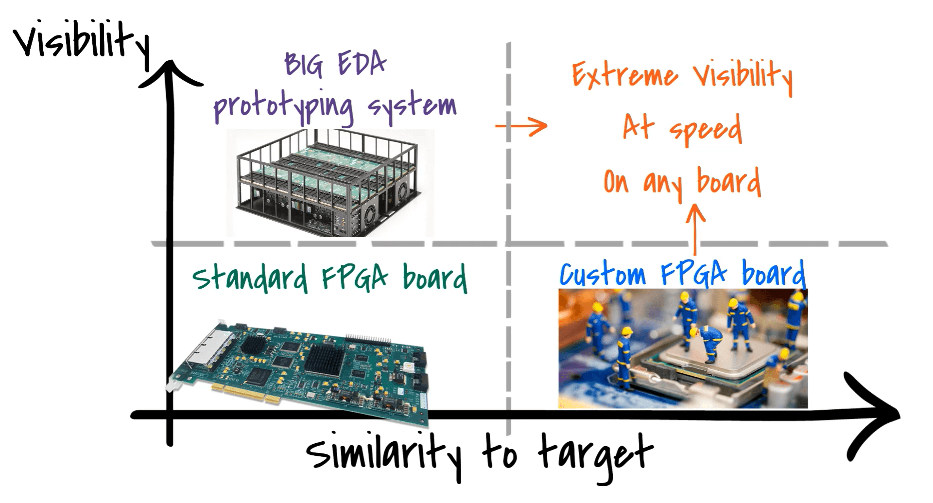
‘Similarity to target’ is the rather intuitive notion that a prototype has to be as ‘similar’ as possible to the target chip. Typically, it means that the ASIC or SoC should be mapped onto one or multiple interconnected FPGA’s connected to peripherals essential to its working. The prototype should also feature the same interfaces as the target subsystem so it can be placed in its target environment as if it were the real chip.
One of the problems with similarity is whether a FPGA technology provides a sufficient amount of gates. When possible, partitioning the ASIC onto a minimum number of FPGA chips minimizes the number of FPGA-to-FPGA interfaces and helps maximize the prototype running frequency.
With FPGA technologies running about as fast as modern ASICs, and up to 40B gates on a single chip, it seems that FPGA prototyping has become easier – it takes less FPGA chips to map a single ASIC.
What we hear from our customers, however, is more contrasted.
It is generally acknowledged that the FPGA vendors’ offering – with extremely complex devices – provide plenty of options for prototyping. The best board is often the one built specifically for a project and based on the latest technology. Buying or making a new board for each ASIC could be budgetary acceptable, but it provides the poorest tools options, often limiting the choice to a few standard tools (maintaining a full line of in-house EDA tools is not really practicable budgetarily in the long run)…
Conversely, investing in a specific board system because it has tools specifically developed for it proves to be a poor choice in the long term: when such a system is purchased, justifying its cost usually requires to re-use it for multiple projects instead of purchasing a new platform (with bigger and faster FPGA’s) when a new chip development is started. FPGA boards get older but do not get automatically or rapidly replaced. Typically, it results in having to use outdated FPGA technology while the ASIC or SoC is faster and more complex. In the end, the prototype does not run at speed of operation any more. So much for the similarity to target…
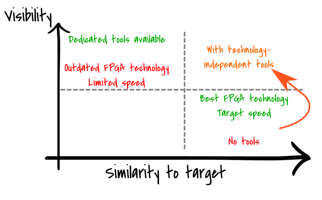
As visibility is paramount in all the tasks that justify the value of FPGA-based prototyping for ASIC and SoC, tools providing extreme visibility no matter the chosen FPGA board allow prototyping approaches that score high both for the similarity to the target AND visibility.
(Worth noting, a generalisation of this approach would put the designer back fully in control of the choice of the ASIC and SoC prototyping.)
In a future post, we’ll discuss about the specific features required for such a tool. Stay tuned!
As always, thank you for reading.
– Frederic