SoC Validation & Debug
Add massive visibility to all FPGA Prototyping platforms.
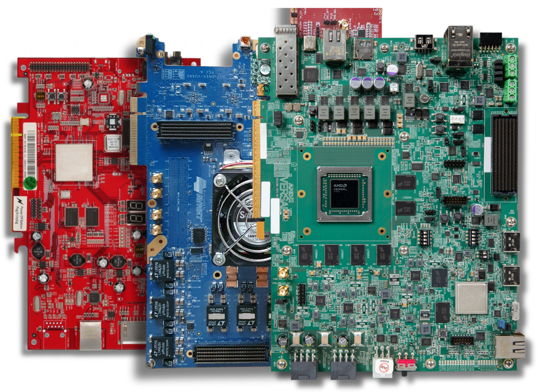
Freely choose or make your own prototyping platform for validation & debug.
Why use prototypes?
FPGA Prototyping is key strategic approach to SoC and ASIC design. We generally use prototypes for the following purposes:
- Design software
- Run the system in realistic environement
- Reach a sufficient number of cycles before production
- Demonstrate IPs and subsystems
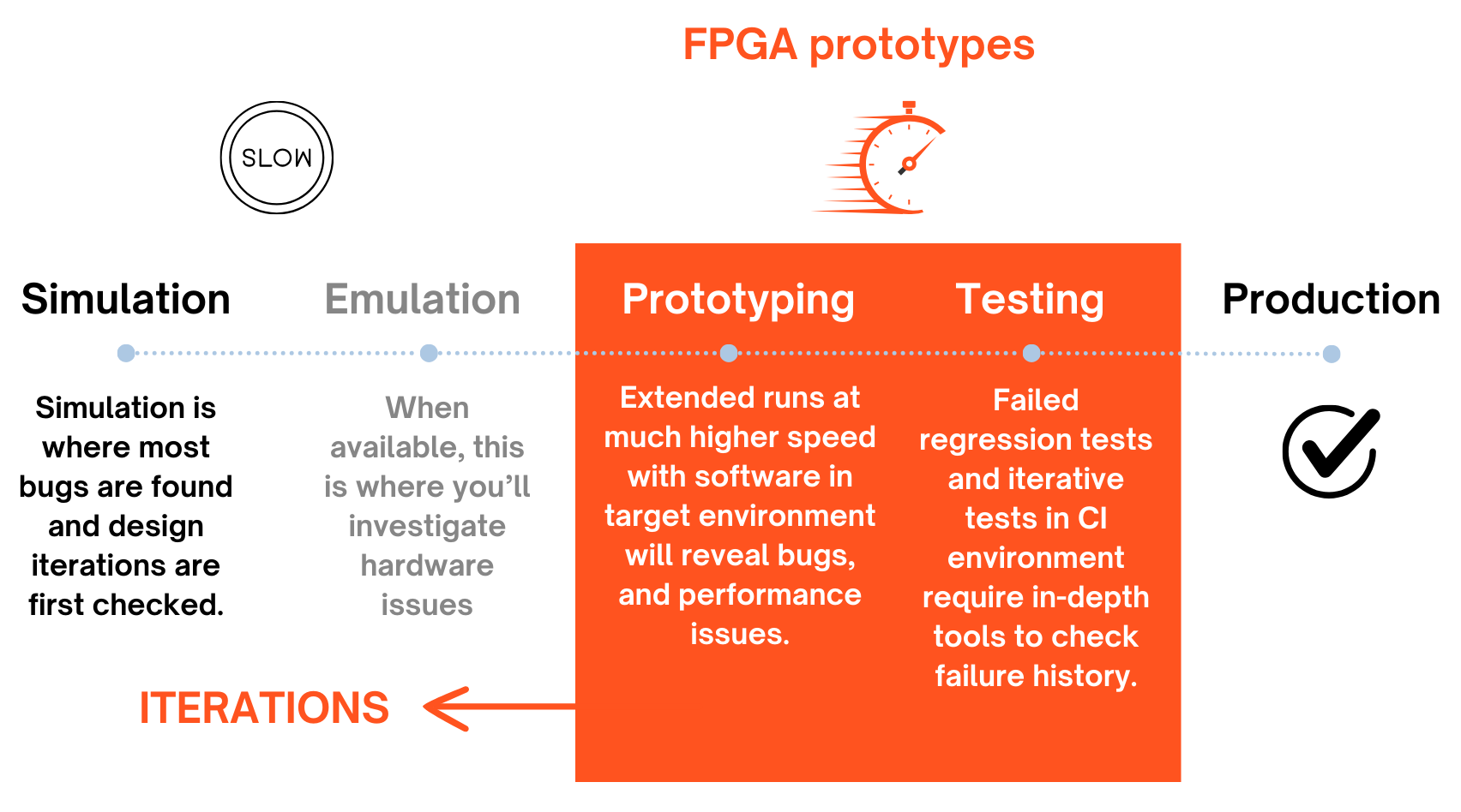
In essence, FPGA prototypes stand out for their proximity to ASIC/SoC gates and their execution speed. They occupy a distinct position that neither simulation nor emulation can fully replicate, as they operate realistically at the environment’s speed without necessitating artificial lowering of test setup speed. They become indispensable up to a critical number of gates, beyond which handling setup time becomes challenging.
When extensively employed for regression or continuous integration testing, FPGA technology can achieve a significant number of test cycles prior to production, bolstering confidence in the thoroughness of the system’s testing.
The Power of FPGA Prototypes in the verification flow
Unlocking the potential of FPGA prototypes is crucial for uncovering a multitude of issues.
Bugs surface during software execution on the assembled prototype. Pinpointing whether these bugs stem from software glitches or hardware flaws demands meticulous scrutiny.
Furthermore, the integration of IPs may fall short of anticipated performance levels, necessitating detailed analysis to identify necessary system modifications. Finally, placing the system in a realistic environment can expose unexpected behaviors, highlighting flawed assumptions and erroneous simulation models.
Addressing these issues involves iterative design and verification processes, usually using simulations or emulation environments. However, their slower speeds and potential oversight of prototype issues highlight the need for precise data collection to ensure efficient iteration.
Exostiv Labs brings visibility in the prototype.
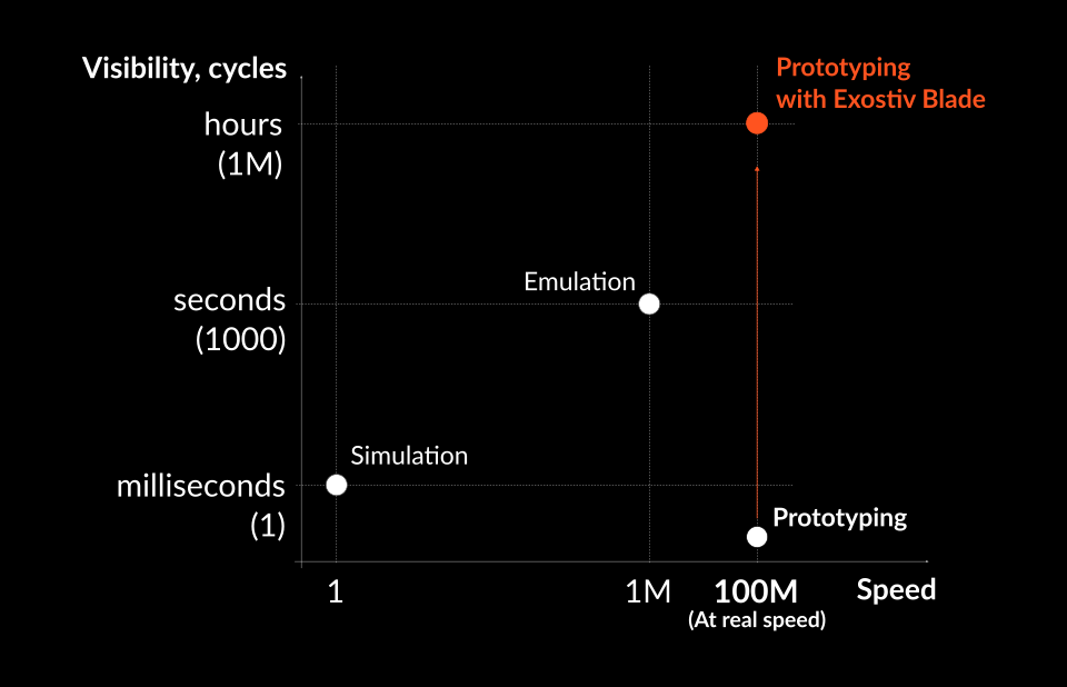
Prototypes have been strong in speed but have significantly lagged behind simulation and emulation for visibility.
Simulation, considered the bedrock of verification, is easily accessible. Yet, due to its slow pace, accurately simulating real-world issues demands careful isolation of the conditions of occurrence. Although emulation offers a potential remedy, it is not always available nor affordable.
With Exostiv Labs, you can reach million nodes and extract ultra deep information from FPGA prototypes
The benefits of ecoupling the tools from the FPGA prototype.
Why we focus on the tools, not the board.
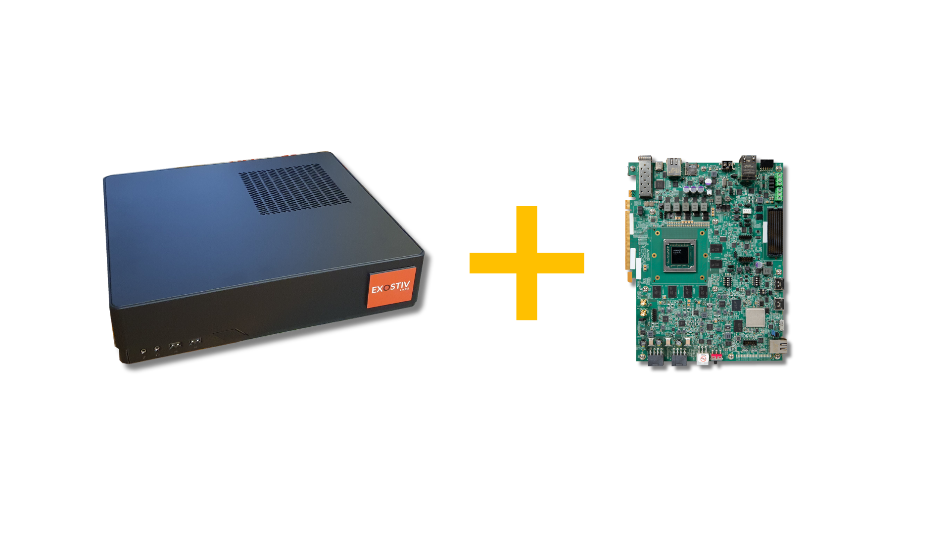
1. Keep your options open
Getting equald visibility performance no matter the target opens up your options when choosing the ideal prototyping platform for your design.
2. Use tools for more scenarios
No matter if the FPGA board is used for debug, software design or system testing, our aplpiances can be used across multiple usages, on all FPGA systems until production.
3. Protect your investment
With a scalable observation platform, the tool can be re-used for a broader range of designs over time. You add or mobilize resources at will and share them with other users in your organization.
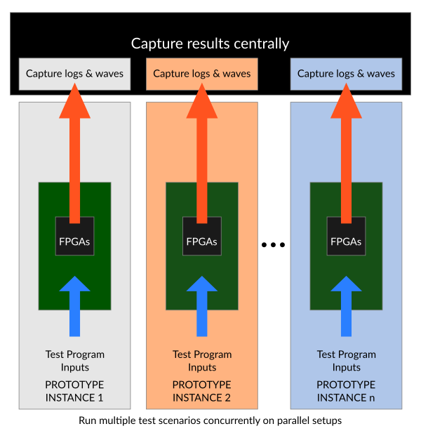
Run multiple concurrent FPGA prototypes
Duplicating prototyping setup and running parallel concurrent tests are the key to augmenting the test density and coverage*
With Exostiv Blade series, you are able to set up a central appliance to capture massive traces from multiple FPGA prototypes. Our solutions adapt to any FPGA board and provides advanced Python scripting for automation and usage with your continuous integration (CI) system.
*Read this article and find out why it is important.
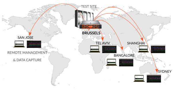
Manage your prototyping assets and have massive FPGA visibility enterprise-wide.