What can Exostiv Blade do for FPGA prototyping?
Classifying FPGA prototyping debug and analysis methodologies.
‘FPGA Prototyping’ or ‘using FPGA boards to prototype an ASIC or a SoC’ can be done with a variety of systems. Using such a system requires additional tools to synthesize and partition the design, and importantly, to debug and analyze it. Most of these tools fall into one of the following categories:
-
External probes: uses external instrumentation products such as scopes or protocol analyzers to run measurements from outside FPGA chips.
-
FPGA BRAM-based logic analyzers: typically AMD ILA or Intel Signaltap. These instruments store traces from the FPGA into internal FPGA RAM, which is then readback through a JTAG interface.
-
Deep trace buffers: this approach extends the JTAG embedded logic analyzer approach and stores the traces to external DRAM.
-
Global State Visibility: this approach consists in running the system clock one clock tick at a time to stop the execution of the FPGA and allow reading back the state of the flip-flops and memory at each cycle, usually through a JTAG interface.
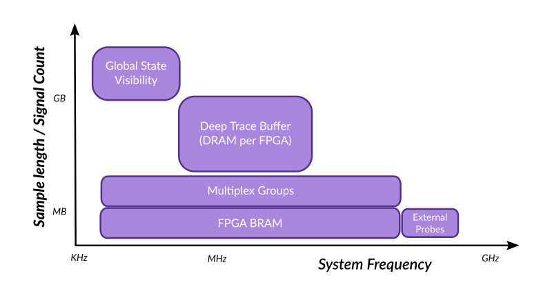
All these techniques have their merits and limitations. They occupy a specific space which are usually summed up with the chart above. We understand that this chart might not be perfect (for instance, why consider multiplexing as a specific type of tool?) – however it constitutes a rather good consensus of how such tools are compared. (This chart was re-created after presentations given by some EDA companies).
The vertical axis of this chart measures the overall capture size, how much of the working system can be observed, which can be summed up as ‘visibility’. As indicated on the axis label, this measure is actually two-dimensional:
-
‘Signal length’: the capture ‘depth’. How many ‘samples’ can be captured and analyzed; in other words how many clock cycles – contiguous or not – does the debug and analysis tool allow to watch?
-
‘Signal count’: the capture ‘width’ or ‘reach’. How many internal signals can be observed?
The horizontal axis of this chart shows the frequency at which the system has to run for the debug and analysis method to be usable.
Reading the chart
For instance, ‘Global State Visibility’ scores high vertically because this technique allows reaching all registers of the system. It scores very low horizontally because this approach requires gating the system clock and run long read operations at each clock cycle in such a way that the system is really used as if it were a succession of ‘static’ states. Conversely, using a JTAG embedded analyzer (‘FPGA BRAM’) provides only a very limited capture width / depth because it uses leftover BRAM resources in the FPGA – and hence scores low vertically. This method works at system speed, however, and can go to several hundreds of MHz – spanning wide on the horizontal axis.
The limitations of Deep Trace Buffer tools
Have you ever wondered why ‘Deep Trace Buffer’ does not score higher in visibility and does not reach system frequency?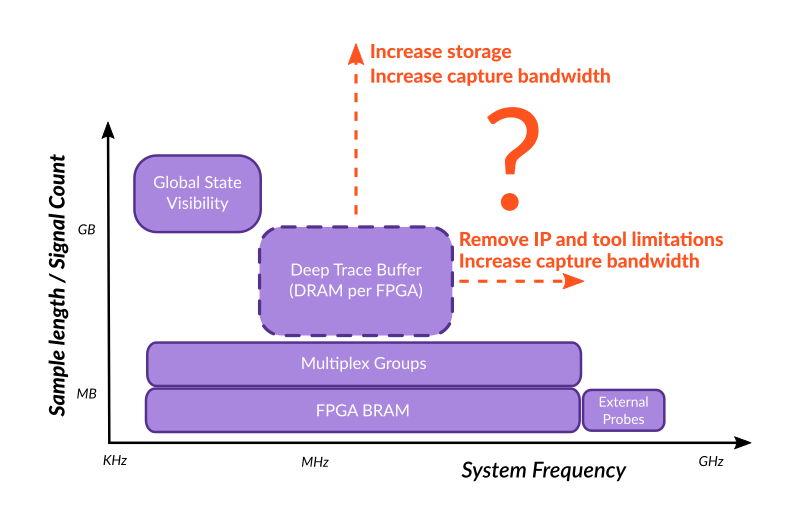
Integrated FPGA Prototyping system usually have the following limitations:
1) Storage size and bandwidth limitations.
FPGA Prototyping systems vendors often claim that they have ‘deep trace buffers’ – DDR SDRAM memory connected to the FPGAs. However, this is insufficient to understand the real capabilities.
Will the quantity of memory available for debug and the maximum bandwidth to it be practical for your FPGA Prototyping scenario? Is this memory resource dedicated to trace buffers or does it have to be shared with the prototype functionality? It is sometimes – wrongly assumed – that a FPGA prototyping system does not have to run at speeds beyond 5 or 10 MHz and hence that the bandwidth to the trace buffer is relatively unimportant.
In many instances, however, FPGA prototyping should run at or close to the target speed of operation, at least partially. An example of this occurs when the prototype includes interface IPs that need interoperability testing so they have to be connected to real external devices that cannot be slowed down. With local system speeds at 500 MHz and more, a high bandwidth to memory turns out to be a requirement in the end.
Hence, what is sufficiently ‘deep’ for your use? 1GB? 8GB? More? How much do you need per FPGA? What will be the target prototype speed and how many signals do you want to observe? These questions are crucial to a successful debugging scenario and you should not just stop with a checkmark in front of ‘deep trace buffer’.
From our client’s experience, we can say that no matter the resources available on a FPGA Prototyping system, there is some level of frustration at some point. Usually, a single DDR memory trace buffer is attached to all available FPGAs, which is not very flexible. It will be ok or far too much for some FPGAs, and insufficient for others, with no way to reallocate the memory that’s physically connected with a fixed scheme (or at the cost of having to send data across multiple FPGAs to reach more memory).
2) Architecture and raw performance of the sampling IP and the software.
How fast can the capture run?
Often buried deeply within the specs of your FPGA Prototyping system is the maximum speed performance of the trace capture. Whether it is limited by the capture IP, the platform software or the physical interface with the buffer memory, you’ll find one that is usually not the maximum speed of the used FPGA technology. Of course, in most of the cases, partitioning a large design onto multiple FPGAs will force you to reduce the overall frequency, because FPGA to FPGA interfaces are used in a time-multiplexed for multiple separate interfaces. For this reason, FPGA Prototyping systems are rarely scaled for at speed operation, and so are the accompanying resources for debug.
Exostiv Blade extends Deep Trace Buffer capabilities
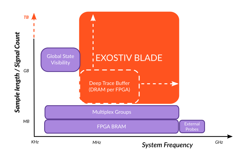
The chart above shows Exostiv Blade positioning compared to the tools currently available in common FPGA Prototyping systems. It extends the ‘Deep Capture Buffer’ capabilities at various levels:
-
First, Exostiv Blade provides scalable DDR memory quantity and bandwidth resources. The user is no longer restricted to the resources available in the FPGA Prototyping system and is able to multiply the memory resources attached to any given FPGA and decide about the available bandwidth. The cost in FPGA resources is primarily the allocation of transceiver quads. The granularity is min. 16 GB of DDR memory per 100 Gbps of bandwidth, and this can scale up to 128 GB per 100 Gbps, enabling very deep capture.
-
Second, Exostiv Blade IP used to sample data from inside FPGAs is able to run up to 800 MHz – currently limited by the FPGA technology. Any Exostiv Blade IP insertion must still reach timing closure together with the overall FPGA design, but does not introduce any arbitrary limitation itself.
- Finally, Exostiv Blade uses a low level protocol on the transceivers that can be scaled easily without bringing a limitation on the available bandwidth. This protocol guarantees over 90% usage of the maximal available bandwidth for trace data payload. For this reason, the structure of Exostiv Blade does not bring any arbitrary software-related limitation either.
Thank you for reading.
– Frederic