Upgrading FPGA Prototyping for High RTL Debug Productivity
The importance of FPGA prototyping
Despite important advances in simulation-based validation and emulation, ASIC engineers worldwide keep on using FPGA prototyping systems. Earlier this year, we have seen the launch of a new generation of such systems from multiple major EDA vendors. These upgrades provide more and faster gates to prototype highly complex chips. Although it might be argued that FPGA might not be the best target hardware for advanced nodes, some of the major EDA companies continue to bet on complex FPGA prototyping systems. This alone is one of the best indicators that simulation and emulation are not sufficient for debugging. And we think that prototypes are still relevant not just because they are cheaper than emulators.
As reported by Rob Parris, from Synopsys: “The problem is that bugs in highly complex chip designs are often buried deep in your system and they will not be found by simulation and emulation alone. They tend to manifest themselves in non-deterministic ways based on complex and unpredictable interactions between hardware and software.”
So, the reality is that creating the conditions that produce bugs requires running software on a prototype hardware, running at target speed of operation (or near to target speed) and running a sufficiently large number of cycles (Interesting read: ‘Deep cycles’ by Bryan Dickman and Joe Convey). This is what a good FPGA prototyping system does well – and the reason for their success, upgrade after upgrade.
Productivity requires properly sized resources
Whether you are designing full ASIC or specific IP, develop software that runs on a SoC or are in pre-production testing, each usage impacts the choice of the FPGA prototyping platform.
1) Does the prototype have to run at full target speed?
- Is it ok to partition the design onto multiple FPGA and reduce the system clock frequency due to the bottlenecks at the FPGA-to-FPGA interfaces?
- Is it possible / affordable to use the most recent FPGA technology to have a better chance of fitting onto a single chip running at max. speed?
2) Is there a clear estimation of the resources needed for observation and debugging?
- How many nodes need to be observed?
- What capture depth is enough?
- How will these needs evolve over time?
3) If the prototype is partitioned on multiple FPGA:
- Is there a need to extract data from *any* of the FPGA used for prototyping? Conversely, will the observation focus on specific parts of it?
- Is it really sufficient to trace and observe the system through its software?
Consequently, target design strongly conditions the choice of the prototyping board (see ‘No one-size fits all’ below) AND the resources required to actually do the job of ‘debugging or testing’. These resources should allow the engineer collect the data that is sufficient to verify if the design works as expected – and if it does not, allow the engineer understand what needs to be fixed.
The debug resources are as important as the FPGA boards
Now you are at the point where you know the context. You have chosen or built a (series of) FPGA board(s) where the target ‘design’ can be fitted and can run at a satisfactory speed to match your needs. You also know what you need to look at to perform the task that you were initially assigned (debugging, verification, testing, software dev, …).
So, what’s next on your list is checking if you have the resources to do the job.
The first questions are purely technical:
- Is there the proper bandwidth readily available to extract the required data from the system at the prototype speed?
- Is there the capability to capture, store and analyze the required data?
If these resources are not available on or delivered with the prototyping system, can they be added?
The second series of questions are partially technical and mostly ‘budgetary’:
- How many FPGA boards prototypes need to be installed in parallel and run concurrently?
- How much of my today’s investment in a prototyping system will I be able to re-use in the future and for how long?
- If my needs evolve over time, will I be able to upgrade the available resources economically rather than having to buy new systems for each project?
Whether you are considering to buy or build a prototyping system, the budgetary consideration will come forward. Saving on CAPEX will always be a requirement, and there are chances that you’ll be asked if you can reuse or upgrade an existing base for multiple projects – especially if there is a large number of units deployed to run concurrently. This is true for the boards, but also for the debug resources.
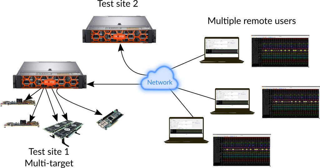
Similarly, it can be desirable to be able to access the prototyping resources remotely, as it reduces the need to duplicate the systems for companies having engineering teams at multiple locations worldwide and working from multiple time zones. There is no doubt that this has become one of the top concerns with the COVID-19 crisis.
What does Exostiv Labs have for me?
Exostiv Labs focuses on providing visibility into the FPGA. Our company proposes a diversified set of (HW/SW) products able to fit to a wide range of needs in FPGA product design, ASIC and SoC desing, IP design, design testing or system software development. Instead of providing fully integrated prototyping systems, our company focuses on the means, tools and resources required to do the most efficient job during test, debug, verification on FPGA systems.
We think that indepedent tools compatible with any FPGA board system has the tremendous value for our clients that it leaves them with the total freedom to choose or build the FPGA platform that best fits to their needs. It is a real ‘niche market’ ambition: being the best in a narrow scope.
Exostiv :
Exostiv is a bench-top non-upgradeable hardware appliance:
- Single FPGA / one FPGA at a time with a single user.
- 50 Gbps bandwidth + 8 GB trace storage.
Typical applications:
- FPGA product debug
- IP prototyping
- Small ASIC prototyping
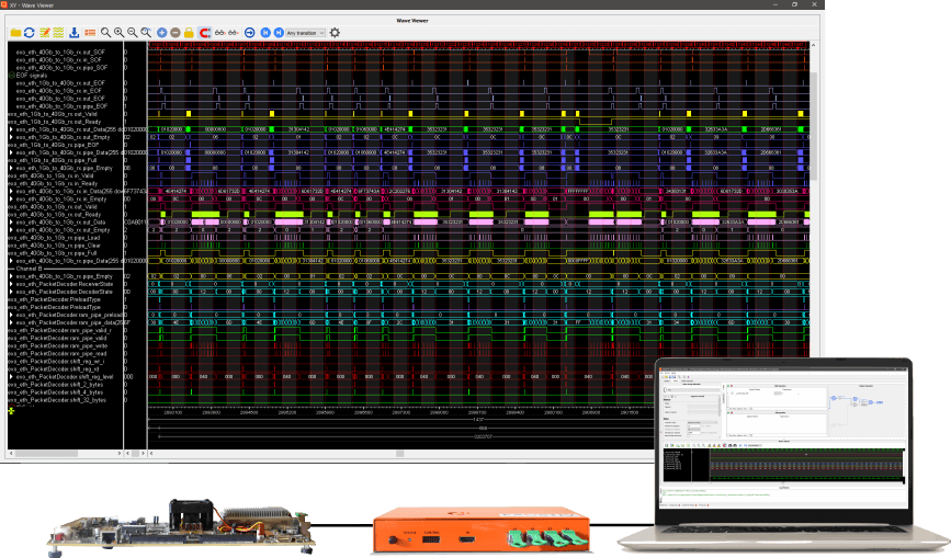
Exostiv Blade :
Exostiv Blade is a remote-controllable & scalable hardware appliance:
- Multi FPGA / Multi board / Multi user.
- 100 Gbps x n bandwidth + 16 GB x n trace storage in various form factors
Typical applications:
- Complex ASIC / SoC prototyping
- Regression testing on multiple parallel setups
- FPGA product debug
- IP prototyping
No one-size fits all!
For instance, testing an interface IP against realistic peripherals requires running the target frequency because you do not want to slow down the environment.
Similarly, when running pre-production testing, you want to run as fast as possible because all testing are time-limited and you want to create as many potential ‘unpredictable’ bug conditions. In that case, fitting the prototyping into one single large FPGA running at up to 500 MHz can be the requirement, which directly impacts the choice of the FPGA board. It is probably equiped with a single FPGA from the most recent generation. The system can be observed through a limited number of FPGA IOs, but this interface must be fast! At 500 MHz, a lot of data is generated each (milli)second in the FPGA. Similarly, capture storage should be deep enough, as the capture memory will fill in quickly.
This use case is *very* different from a ‘general purpose’ ASIC prototyping, where the user mainly seeks accelerating the execution of typical cases that he would otherwise have to run in simulation: the speed does not really matter, as running the FPGAs at 1 MHz or 5 MHz is already considerably faster than a simulation – and the user won’t focus on specific IPs but needs to look across the whole design. Stopping the clock to capture internal states is equally acceptable and applied as a technique too. Consequently, debug data will have to be captured from multiple FPGA / multiple ports, potentially triggering each other. Taken individually, each observation interface does not have to be especially fast or have deep capture capability, but the aggregated bandwidth and storage resources can have to scale, as more ‘gates’ of the target system need to be observed.
As always, thank you for reading
– Frederic