10 things you should know before SoC Validation
1. Validation and verification are different things
2. Emulators do not replace prototypes (and the other way round)
3. There are silicon bugs left to be found during validation
4. Design size matters
5. Each FPGA size matters
6. Speed matters
7. Number of cycles in service matter
8. Validation is a multi-faceted job
9. Not all IPs are equal
10. Tools real capabilities matter
1. Validation and verification are different things
Both verification and validation are used to check the design ‘correctness’ – they however answer different questions:
– Validation : ‘Are we building the right system‘?
– Verification : ‘Are we building the system right‘?
So, the fundamental difference is that validation determines that the system (product, …) meets the intended usage. In contrast, verification checks whether the system meets the specification.
Verification vs. Validation – a real-world example.
A few years ago, our company was involved in design activities and we worked for a client that made video broadcast equipment. We were in charge for the design of a FPGA that processed multiple 4K video streams destined to be displayed on specific screens considered to be the standard in their market. Formally the specification required from the processing to generate 4K SDI video streams with various formats after processing.
The specification of such video streams is well documented and after design, we could run simulations to verify that the processing was compliant to this specification in all of the chosen modes. Then we decided to place a prototype of this system under realistic conditions and output our video streams onto the reference 4K display.
Some modes did not work at all.
After analysis, we came to the conclusion that although the display was considered as the market reference, it was not fully compliant to the 4K SDI specification we had received. We have had to tweak the video generation algorithm to optionally support the way such displays expected 4K SDI video streams.
In this case, using a prototype has allowed us validate whether our design would meet the intended usage: after consulting with our client, it had become clear that the system had to support the market standard type of display, even if it required from us to implement a modified video stream that was not compliant to the 4K SDI standard.
2. Emulators do not replace prototypes (and the other way round)
We sometimes receive the feedback that ‘everything’ (verification?) is done with simulation and emulation – or that using an emulator makes prototyping useless.
In cases prototyping is practicable we think that this is a confusion between verification and validation: – Like simulation, emulation is model-based. Such models potentially originate from an incomplete, flawed or imperfect specification. And even with a ‘perfect’ specification, models can have errors. For these reasons, relying on models only and skipping tests under realistic condition seems to be an adventurous bet. – Emulation is nowhere close to the target system speed, even if it is faster than simulation. Emulators have a lot of advantages, but cannot get you close to realistic speed conditions.
– Part of the validation consists in checking the performance with a SoC software execution. Due to the model usage and the speed limitation of emulators, it is often impractical to run the target software on an emulator. – Interoperability with external equipment is difficult to validate with emulators: real equipment are what they are (= sometimes imperfect). You cannot usually slow them down, as functioning ‘in the field’ means at the speed that they are built for. This disqualifies emulators for such tests.
Validation has to be done, somehow.
How is the system tested as a product? Pre-silicon or post-silicon? There are cases where the drawbacks of building a prototype exceed the advantages of using them. For instance, some systems are so complex that they have to be parititioned onto hundreds of FPGA chips, leading to a tedious process of building the prototype and sluggish speeds anyway. So, prototyping is not for everyone. When it is possible, however, the cost of building and using it will be much lower than the multi-million cost of a re-spin.
3. There are silicon bugs left to be found during validation
Debug and verification do not end when validation starts. The hard truth is that finding the next bug is exponentially harder. Hence, finding it faster means you need to work with a faster system.
Consequently, you should make the most of all steps. Validation with a prototype is an opportunity to make verification more complete. So you need to prototype – and do so with the ability to observe the system at the right level.
Your verification is as good as what you put in it
Over the last decade, verification metholodogies have tremendously evolved, and seen the widespread adoption of techniques such as UVM. Teams that have successfully implemented it have seen quite some benefits – mainly in their ability to formalize the process of verification, work in teams and specialize the job of doing verification.
However, we should not be fooled by a perfect scorecard or a perfect coverage, as verification does not reduce to learning advanced programming techniques and executing them right. No matter if directed testing or UVM is used, the efficiency of the chosen verification methology is as good as what you put in it.
In its recurrent survey, Siemens EDA shows it: bugs still escape to production despite the now widespread adoption of advanced verification techniques. Some bugs won’t practically be seen during verification. You need something else to find them.
4. Design size matters
Recent numbers show an adoption of 39% for FPGA prototyping vs. 23% for emulation. Interestingly in the same survey, FPGA prototyping dominates emulation for ASIC designs up to 1B gates. Over 1B gates, emulation takes on prototyping.
It seems that 2 factors explain this situation: – On one hand, ‘smaller’ design (< 1B) verification can be managed without emulators. Accelerating simulation with emulators does not always justify the investment in such costly devices.
– On the other hand, the difficulties in setting up a usable FPGA prototype to validate very large designs can outweigh the benefits of this approach. For instance, partitioning very large designs onto hundreds of FPGA chips can lead to impractical setup times and sluggish speeds that diminish the interest of FPGA prototyping.
The efficiency of pre-silicon validation on FPGA prototypes has a sweet spot for small to mid-size designs that can be partitioned on 1 to 16 FPGA chips. Beyond, this point, an hybrid approach that combines emulators with some IPs mapped into FPGAs could well be a better way to go.
5. Each FPGA size matters
Partitioning ASIC or SoC onto multiple FPGA chips makes prototyping more difficult and less realistic. The overall running frequency of the prototype depends on the partitioning process because some signals are serialized at the cross-FPGA interfaces. Consequently, FPGA prototyping system often run at no more than 10 MHz for systems having to run in the 100’s of MHz in the field – or even GHz. Consequently, the less you need to partition, the more realistic the FPGA prototype.
Ideally, interface IPs and key specific subsystems of the ASIC should be mapped onto a single FPGA chip. This allows running at least this part of the prototype at a speed close to realistic speeds – and enable interfacing the external world without having to find a trick to ‘slow down the environment’.
When defining a FPGA prototyping platform, you should not just checkt he total number of gates available, but the size of each FPGA chip as well. Using the most recent technologies will enable you to run at potentially higher speeds as well.
6. Speed matters
Using the fastest prototype is required for productivity as realism. We are not discussing a case of having to use a prototype instead of an emulator or a simulator. You probably need all of them.
A faster prototype makes a difference for your ability to explore validation test scenarios. So, yes, 500 MHz is (50 times) better than 10 MHz. Parallelizing – that is using multiple setups simultaneously – can be an efficient way to reach the same goal – even better, shall we say.
Beyond productivity, one of the advantages of a speedy prototype resides in its ability to realistically reproduce the conditions of operation of the system once produced. Immersing the prototype into real-world stimuli (such as when you test the interoperability of the prototype with real world equipment) requires running at realistic speed of operation. You rarely are able to easily ‘slow down’ the environment.
The truth is that in some cases, you just need 500 MHz. Period. And that applies to the capabilities of the validation tools too.
7. Number of cycles in service matter
Once a SoC is produced, sold and in service in the field, it will quickly execute cycles. A lot of them. A single GHz processor running during 1 hour is already in the 10^12 number of cycles. And there will be millions of them over many years of lifetime. Consequently, there is basically no way to run all combinations of usage prior to production. You can get close to what seems to be sufficient with a prototype – but even then, you’ll be far from the count.
The bottom line is – you still need to get to a number that provides you the best chance to have caught 99% of the few remaining bugs left after verification. Hence, the total number of cycles that your prototype instances run is important.
For a more detailed discussion about this, we invite you to read the excellent article from Bryan Dickman and Joe Convey: ‘The quest for bugs: “Deep Cycles” (Approximating Silicon with FPGA Prototyping).’
8. Validation is a multi-faceted job
You have a prototype that you can use for validation. It is immersed in a realstic environment. Now what?
Well, you need to define test scenarios and stimulate the prototype to run the tests. As you’ll repeat this, you will need some controlability and flexibility. So, you’ll use some form of software to build up your tests scenarios and run them. Great.
Then you need to know if the prototype provides the expected test result. Does the system exhibit the expected behaviour? The expected level of performance? So, you’ll need to somehow measure the test’ results and define a PASS/FAIL criteria. Using software is again a flexible way to measure this. In addition, the test software can generate execution logs. With a definition of the expected log, you can rather automatically execute the tests and check if they pass.
Now, what if a test fails? What if the result is unexpected?
It is really a ‘forensic’ job – a ‘post-mortem’ analysis of what happened.
Potentially, it requires to look into the prototype at many levels:
- Software logs
- Software detailed execution
- SoC structure / bus-level
- Inside the SoC IPs
- …
The bottom line is that validation requires an extended toolbox of software and hardware tools that build on the prototype capabilities. Without this toolbox, the validation engineer is basically blind.
9. Not all IPs are equal
Validation usually happens after verification. The IPs used in the SoC are supposedly functional, verified and compliant to the specification. However, it is worth asking what you built the SoC on. What level of confidence do you have about the IPs verification process? What does it tell about the ability to integrate in a SoC and run well in its architecture? Were the IPs already used in a similar context and are they able to reach the desired level of performance?
IPs might need a separate and specific validation process before they are tested in the SoC taken as a whole.
10. Tools real capabilities matter
As described above, validation is a multi-faceted job, that uses the capabilities of the prototyping system to run test scenarios and capture results. When a test fails or a bug is encountered, it is required from the validation engineer to investigate the failure so he can inform the design and verification team – or possibly the software team – to ultimately fix what’s wrong.
Most FPGA prototyping platforms are delivered with tools that allow looking into the prototype FPGA chips during or after operation. These tools generally fall into one of the categories described here.
Beyond the tools categories, their *real* capabilities are extremely important – and you should always ask about them:
– Maximum speed of operation: is there a maximum frequency of operation for deep trace capture tools? It is commonly accepted that a FPGA prototyping platform for SoC, that runs at 10 top 50 MHz is a ‘fast’ platform. Consequently, it happens that the tools provided with them cannot run much higher than these speed – as it is considered as a useless optimisation. Now, what if you need operation at 500 MHz and beyond? There are chances that properly partitioned parts of the design can run at this speed – as current fPGA technologies can reach this performance level. What about the tool? Does it allow sampling at real speed of operation?
– Impact on Resources: except for the ‘total visibility’ category, most tools require some resources of the FPGA platform. Logic, memory, I/Os, … But what is the actual footprint and what are the options to tune the resources usage? Some deep trace buffer tools claim being able to reach all system nodes without the need to recompile. That’s a great feature, but what is the real impact on the resources? Can you afford this? Will it be practical for you? No matter how you turn the problem around, reaching nodes for sampling requires some logic and routing resources.
– Resources sharing: some deep trace buffer share the same memory and controller resources as the prototyped target application. Check the constraints of this. Are you allowed to run trace capture at an arbitrary speed or is this conditioned by the prototype? Do you have enough bandwidth to use the DDR for the target application AND the trace storage? How about the memory depth made available for debug?
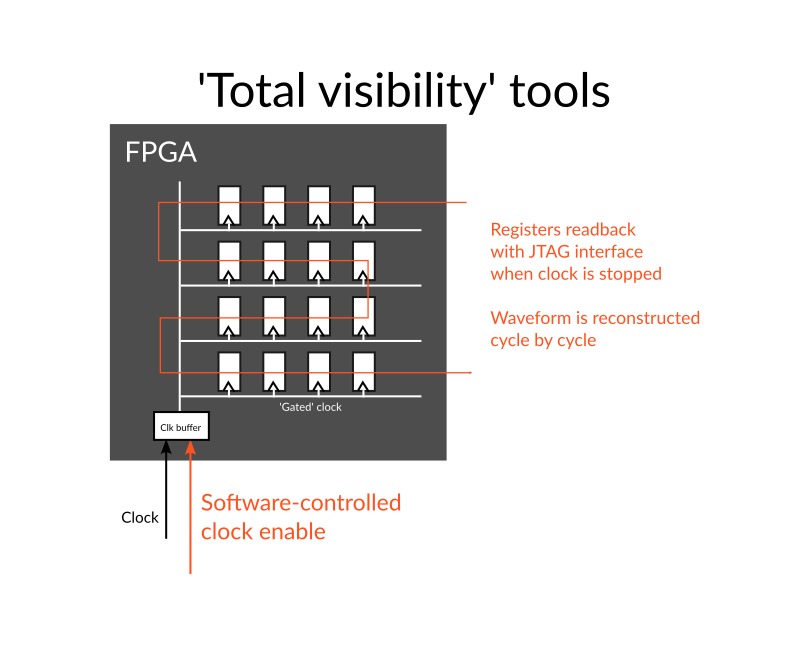 ‘Total visibility’ tools stop the prototype clocks at each cycle to allow reading back the state of the registers and memories in the prototype FPGAs, usually with a JTAG port. This approach provides a high visibility into the chips (as virtually every bit can be readback) and is sometimes completed with the algorithmic reconstruction of some data to avoid having to read complete logic trees. This approach is very slow, and cannot be applied to realistic environments because of the need to stop the environment together with the prototypes. It is more a complementary verification technique to use in comparison with simulation than a real ‘validation’ technique.
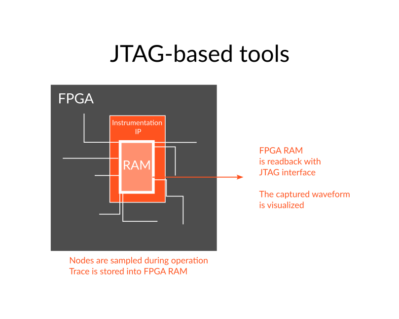 JTAG-based tools – or JTAG embedded logic analyzers (AMD ILA, Intel Signal tap and others…) are relatively lightweigh and universally available (sometimes even for free). Because they store data into the FPGAs blockrams left after the design is mapped, the information provided by such tools is very limited – and often insufficient for advanced validation approaches.
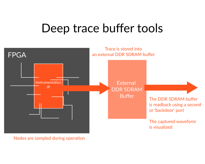 Deep trace buffer tools use a memory located outside the FPGA chips to store trace data sampled from inside the FPGAs. Like the JTAG tools, the advantage is that the traces are captured at the prototype speed directly from inside the chips without the need to stop the prototype execution. Unlike JTAG tools, using external memories enable much deeper trace captures (hence the name), often in the MB or even the GB/TB range. Exostiv Labs has developed a comprehensive series of deep trace tools that bring massive visibility into any FPGA prototype at speed of operation.