You can’t fix what you don’t see

Whether you’re designing a single IP, an FPGA-based product, a CPU coprocessor, an ASIC, or a System on Chip (SoC), your product must work as intended—ideally flawlessly, though “good enough” often applies.
The process starts with a spec, which is usually incomplete or unclear. Then comes design, where you implement the spec, followed by verification to ensure the design aligns with it. Software development runs in parallel, interacting with the hardware. Next is validation, testing the system under near-real-world conditions.
Problems can arise at every stage:
- Specs may be inaccurate or incomplete.
- Designs can have errors or misunderstand the spec.
- Hardware and software may not meet performance expectations.
- The final product might not fit the intended application.
Throughout this process, various techniques come into play. During design and verification, simulation is used extensively, often alongside code coverage and methodologies like UVM, or even formal techniques to ensure the implementation fully reflects the spec. Emulation speeds up this process, serving as a faster alternative to simulation. Prototyping (and sometimes “fast emulation”, whatever that means) becomes crucial when software is added since simulation and emulation alone are too slow for practical software execution. Prototypes are also used in the validation stage when testing the system in a real-world environment.
Anyone in digital system engineering will recognize this workflow. Of course, the specific techniques used depend on budget and complexity trade-offs.
Interestingly, none of the techniques mentioned are explicitly designed for “debugging.”… And yet, they all end up being used for it.
See below, we have tried to represent the position of each technique on a chart.This chart shows the max accessible for each dimension – reaching a specific combination of reach / speed value depend on the case.
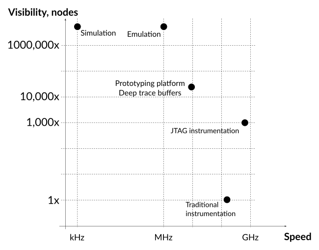
Technique | Max. speed | Max. reach (nodes) |
Simulation | kHz | All (n x 1,000,000) |
Emulation | MHz | All (n x 1,000,000) |
Deep trace buffers in proto platforms | m x 10 MHz | n x 10,000 |
Traditional instrumentation | m x 100 MHz | n |
JTAG instrumentation | 800 MHz | n x 1,000 |
“Debugging?”
Debugging isn’t a straightforward process because a “bug” can refer to many different issues. For example, if a specification doesn’t account for a particular real-world scenario, a verification engineer could verify that the design perfectly matches the spec, yet the spec and design would still need updating to fix the oversight. Similarly, a design might be structurally and behaviorally correct but fail to meet performance expectations in real-world conditions. Lastly, the system environment could be misunderstood or misrepresented, and unexpected combinations of events might cause a system crash, revealing a deeper issue.
As you can see, bugs can occur at different levels, have varying effects, and may require different methods to identify and fully understand them.
However, the one thing all bugs have in common is that they cannot be fixed if they aren’t observed in the first place.
The role of FPGA
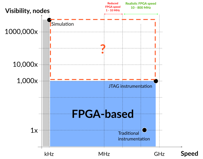
FPGAs play a unique role in the design process because certain techniques require operating speeds in the MHz range to be effective.
Let’s step back and leave emulation and commercial prototyping platforms out of the picture for a moment. These high-end tools, often provided by large EDA vendors, are expensive and beyond the reach of many engineering teams using FPGAs.
Instead, the most commonly used tool is JTAG instrumentation. It’s popular because every FPGA chip has a JTAG port built in, and the necessary tools are already included in the FPGA vendor’s software suite.
Along with simulation, JTAG instrumentation is often all that’s available to help visualize and debug issues. However, as shown below, this leaves a significant gap in the range of cases that can be explored. Many scenarios can’t be simulated because they would require months of runtime. Moving to an FPGA prototype can solve this by allowing enough cycles to be executed, but it usually comes at the cost of limited visibility into the system. As one of our clients put it, “It’s like looking at a complex system through a straw.”
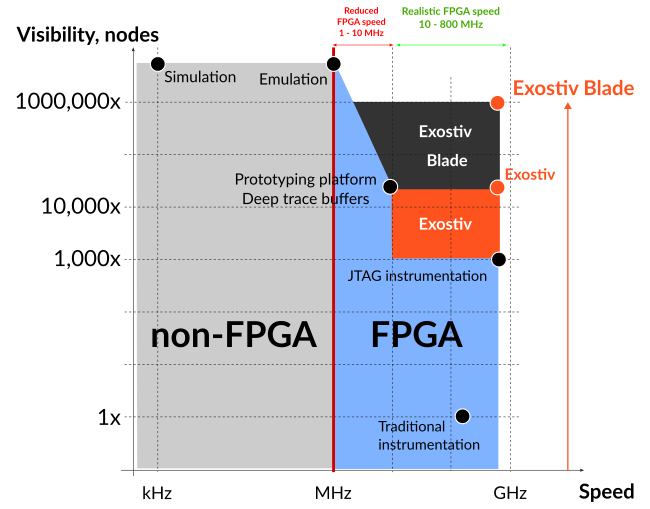
Placing Exostiv Labs products on the map
Exostiv Labs products are able to reach the following max. specs, occupying a space that is shown on the updated chart below.
Technique | Max. speed | Max. reach (nodes) |
Exostiv | 800 MHz | 65,000 |
Exostiv Blade | 800 MHz | 2,600,000 |
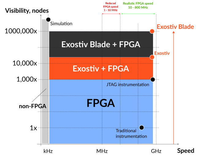
Once you have an FPGA board or prototype set up, adding Exostiv or Exostiv Blade to your existing toolkit opens up a whole new range of exploration possibilities.. That also the case, even if you have access to a more complete set of equipment – see below.
[divider]
Conclusion: plan your debug strategy – with the right tools.
One common mistake today is planning for design and verification but not for debugging. The first priority should be giving yourself the tools to observe your system — after all, you can’t fix what you can’t see. Without expanding your ability to visualize what’s happening inside your system, productivity will suffer, and you’ll waste weeks chasing down elusive issues. Breakthroughs come from observing the system clearly.
Another mistake is dismissing a technique just because it isn’t perfect. Even the most rigorous design methodology and ingenuity won’t prevent bugs. The key is to make the most of every phase of design and take a practical, pragmatic approach.
It’s wrong to think that one technique will solve all problems, just as it’s wrong to avoid planning for debugging because bugs are unpredictable. Debugging should always be part of the plan, with a range of tools and methods that focus on giving you clear visibility into the system.
Exostiv Labs is all about giving you clear visibility into your FPGA platform.
Thank you for reading.