Defining targets (for FPGA debug)
I recently attended a technical seminar organized in The Netherlands by one of the major FPGA vendors (hint: it is one of the 2 top vendors among the ‘4 + now single outsider’ players in the very stable FPGA market). During the lunch, I had the opportunity to discuss with some engineers about FPGA verification. Beyond high-level definition techniques, simulation and other ‘pure-software’ techniques, they all used ‘real hardware’ for some of their verification iterations.
There seems to be a strongly entrenched habit of the FPGA engineer: we cannot resist to the appeal of being able to reconfigure the FPGA indefinitely and try a system ‘for real’.
Yet, for those who would still believe it, the days of simply throwing a design to a board without prior verification are over and for good (check this article for instance). Separate IPs and separate groups of ‘functionally-coherent’ IPs really go through all-kinds of pre-hardware validations.
Like one of my lunch companions said: ‘This is when we put things together for real that virtually *anything* can go wrong.’.
So FPGA Engineers like to go on real hardware for debug. When asked about what they use at this stage of the design flow, the answers are (unsurprisingly?) similar. Two techniques still prevail: either they connect a logic analyzer to some of the FPGA’s I/Os – or they use an ’embedded logic analyzer’.
Traditional vs. Embedded logic analyzer
These two approaches are summarized below (click on picture to zoom):
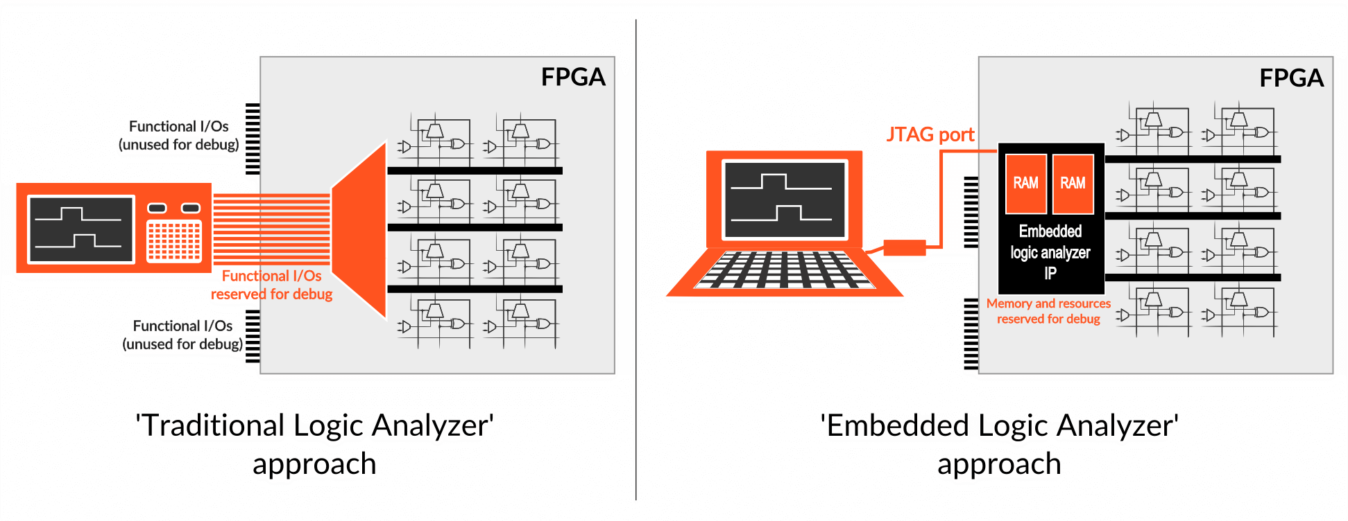
Schematically, using a traditional logic analyzer to debug FPGA consists in making a special FPGA configuration where internal nodes are routed onto some of the chip’s functional I/Os. These I/Os are ‘physically’ routed on board to a connector on which the logic analyzer can be hooked. This approach uses the ability to reconfigure the FPGA to route diverse groups of internal nodes to the same set of physical I/Os. Multiplexing groups of nodes helps reducing the number of FPGA synthesis & implementation iterations. The observed nodes evolution is stored into the logic analyzer’s memory for further analysis.
Conversely, using an embedded logic analyzer consists in reserving FPGA memory resources for storing the FPGA nodes evolution. Subsequently, this memory is read by using the device’s JTAG port. The collected traces can be visualized on a PC – usually in a waveform viewer software.
Which technique is preferred?
This is a usual trade-off between which resources you are able to mobilize for debug and the achievable debug goals.
The embedded logic analyzer is generally preferred because it does not reserve FPGA I/Os for debug. Having a sufficient number of such I/Os for debug can lead to choosing a more costly device ‘only for debug’ – which usually proves to be difficult to ask to your manager.
Conversely, the traditional logic analyzer is preferred over the embedded logic analyzer because of its larger trace storage (Mega samples vs. Kilo samples).
Over time, additional considerations have appeared:
– With FPGA commonly running at more than 350 MHz, signal integrity and PCB costs problems arise when routing a large number of I/Os to a debug connector (trace length matching, power and space issues). This goes in favor of the embedded logic analyzer (not speaking of the much larger price of a traditional logic analyzer).
– In my previous post, I evoked the gap that may exist between the order of magnitude of the memory that’s available in a FPGA and the quantity of data that is necessary for debugging efficiently.
Exploring the solutions space
Supposing that none of the above techniques is satisfactory, how can they be improved?
The picture below shows the relative positions of the logic analyzer and the embedded logic analyzers on a 2 axis chart. It shows the FPGA I/O and memory resources that have to be mobilized by each technique.
The area occupied by each solution shows the relative order of magnitude of the trace memory they provide – which is a good measure of the provided ‘observability’.
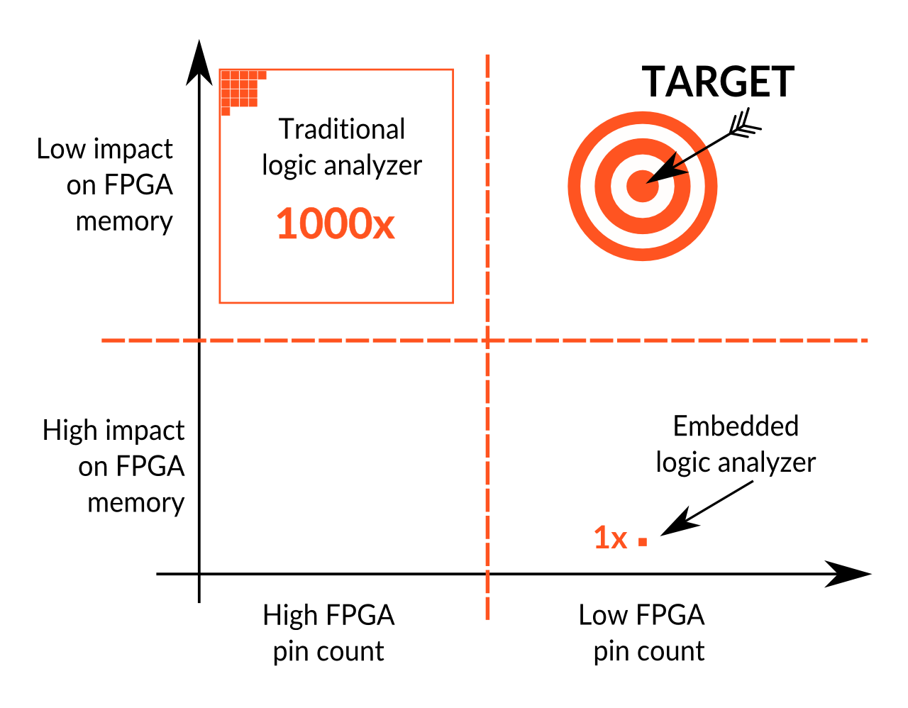
A better solution should:
1) hit the TARGET position on the chart – and –
2) provide even more observability
In my next post, I’ll come back on the impact of reaching the target defined above. Stay tuned.
Thank you for reading.
– Frederic