Delivering High Quality Semiconductor IP with confidence
Because they are the essential building blocks of modern ASIC and SoC chips, semiconductor IPs are used in a wide variety of environments, in which they are in service during extended times.
Verifying that they run flawlessly in all these contexts is not an easy job: the core functionality must be verified in numerous integration contexts, at various speeds, and for interface IP, interoperability with – sometimes flawed – external equipment must be checked.
Reaching these quality targets requires including FPGA prototyping in the verification strategy:
First, FPGA prototyping allows running the IP in a realistic I/O and speed environment that other techniques like simulation and formal verification cannot match. Models are flawed. The environment specification is incomplete most of the time. Placing the IP in its target environment complements the verification with hard facts and measurements – which are sometimes totally unexpected.
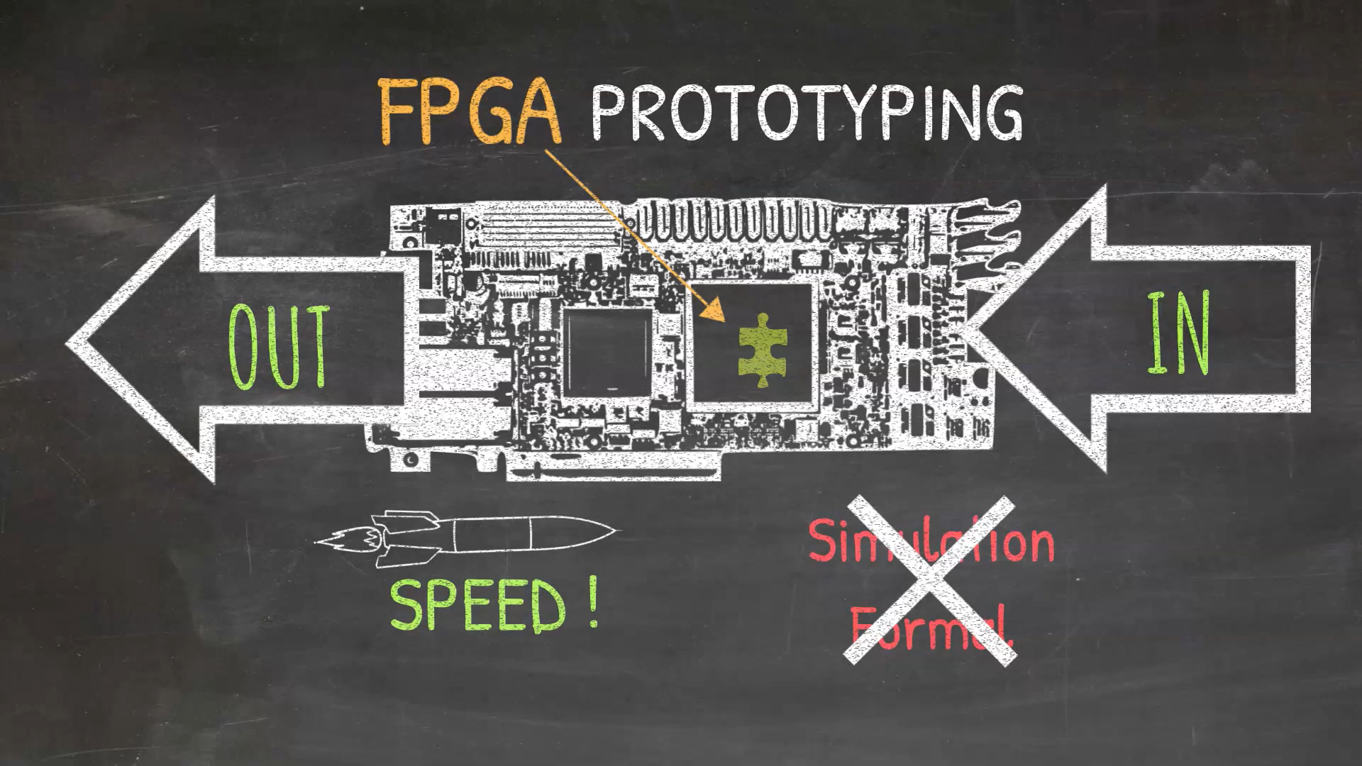
Second, only FPGA prototyping provides a way to realistically reach a sufficient number of cycles in service that allows signing off the IP design with confidence.
Millions of units of the same actual device running in the GHz range are potentially in service during many years. The aggregated running number of cycles can be in the ‘exacycles’ (1e18). Of course, it is impossible – and very cost ineffective – to run as many cycles before releasing an IP. However, getting close to this cannot be done with anything but a (FPGA) prototype.
For instance, if a prototype runs at 20 MHz, using 50 instances of it in parallel gets you close to the equivalent 1 GHz throughput. At 200 MHz, 5 of them are fine. At 500 MHz – … well you get the idea. Comparatively, a simulation reaching 100 Hz performance would require 10 million hours for 1 hour of a GHz IP (or 10,000 hours for 1000 simulations in parallel, assuming you have this processing power). Emulators are better than simulation but you’ll need them in larger numbers than FPGA prototype instances, which can be a tad too expensive – especially for a single IP.
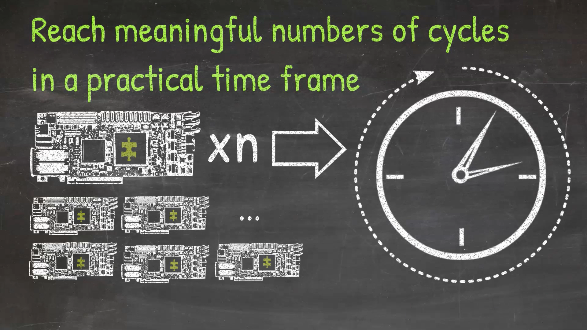
Hence, using multiple FPGA prototypes is a realistic plan for IP verification and must be considered.
Now, the next question is…
Assuming that a bug occurs, are you able to detect it and analyze it?
Unfortunately, making or adopting a FPGA prototyping platform often receives all the focus. However, the prototyping approach remains mostly useless if it cannot provide actionable data when bug occurs or when the IP does not meet the expected level of performance. Therefore, it is equally important to detect issues and collect the information required for correction.
What would an IP prototyping setup be like?
It would be composed of a series of FPGA boards. Each board would provide sufficient FPGA resources (understand: gates, memory, I/Os) in one or multiple FPGA chips to contain the tested IP and some of the testing environment. A local microcontroller is probably required to enable software controllability of the tests, as well as a basic system-on-chip infrastructure implemented in the FPGAs so the IP is tested in a realistic integration environment. On these boards, clock frequencies and other parameters should be controllable as well. Finally, the FPGA boards have to be connected to the required set of external peripherals and interfaces to place the IP in its target environment.
Importantly, the prototype provides the resources used to make measurements and log key indicators. When these indicators show a failure or a bug, these resources have to be able to trigger a ‘post-mortem capture’ from the IP.
It is hard to generalize how these indicators and captures should be. The logs need to provide accurate and complete data to avoid false bug detection. The capture needs to provide sufficient information so the issue can be analyzed and usually easily reproduced in a simulation for final analysis and correction. In addition, this capture will have to be taken from inside the IP, as simple measurements outside of it (or, worse, from outside the FPGA chip) won’t provide actionable data.
So, you need DATA to detect bugs and DATA to correct bugs.
The table below lists the requirements of the IP verification infrastructure in a FPGA prototype:
Feature | Rationale |
At speed execution | IP prototyping is ideally tested at target operating speed in environment. Data should be sampled at speed and extracted on the fly. |
Bit-level resolution inside the IP | Detection and post-mortem capture should provide maximum resolution inside the IP logic for accurate detection and resolution. |
Deep capture capabilities | ‘Post-mortem’ analysis of a bug requires going back to the initial cause of it. The required depth can exceed Gigabytes. |
(Automated) post-processing capabilities | Measuring the performance of the IP and assessing whether it works properly can require algorithmic post-processing of the captured data and logs. Including this capability into the prototype infrastructure is a plus. |
Scalability | Should be able to support multiple FPGA chips in a single prototype and multiple prototyping boards instances used in parallel to expand the overall testing capability of a single IP. |
After analysis, the above requires primarily translate into:
A solution embedded in the FPGA(s): captures must be done at the heart of the IP.
- Bandwidth resources: a lot of logging and analysis data has to be extracted at speed of operation.
- Storage resources: a large history or observation window is desirable to ease analysis and bug fixing.
- Scalable resources: to support multiple FPGA and target boards.
- Data post-processing resources: to ease analysis and data reuse in other environments (such as simulation).
Exostiv Blade meets these goals.
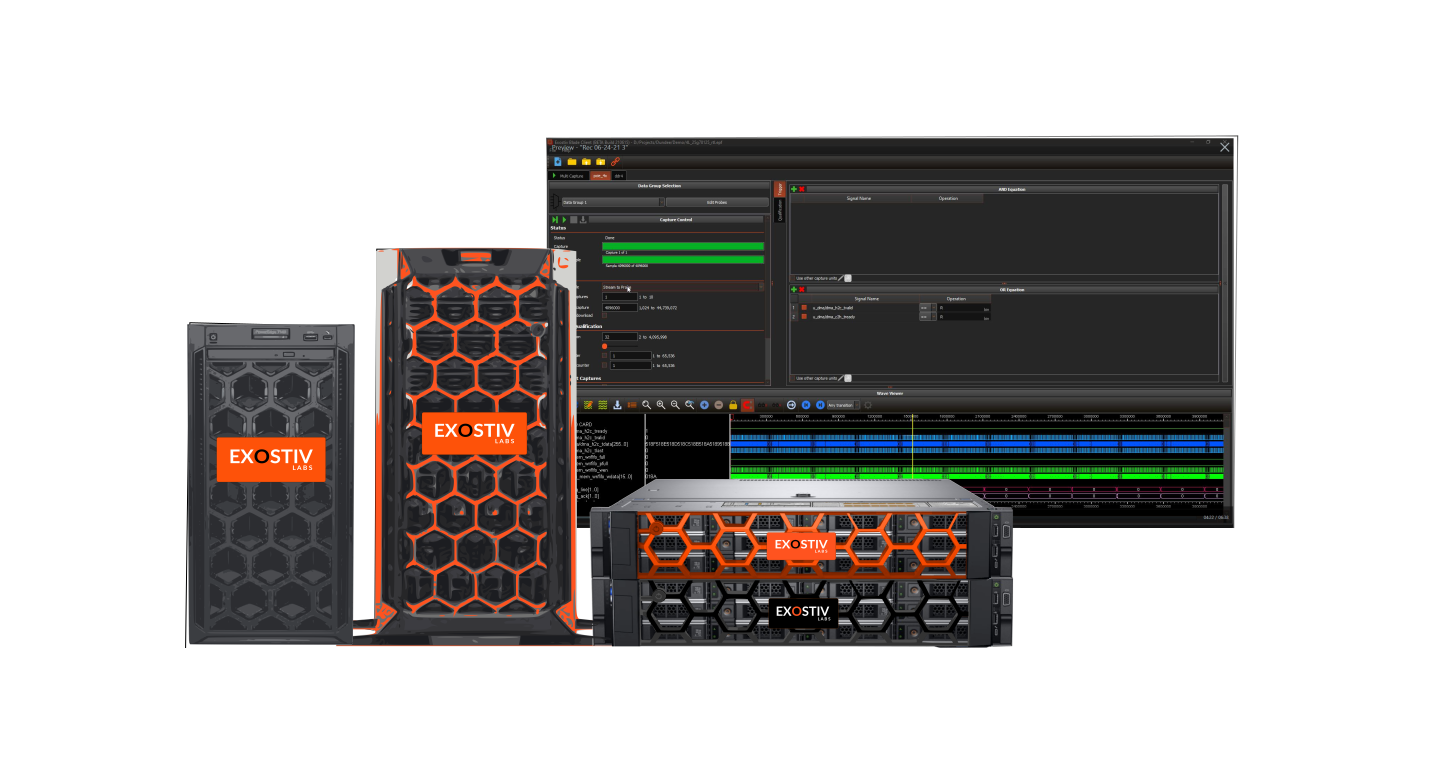
Exostiv Blade uses dedicated hardware based on a client-server architecture used to extract data directly sampled from inside single or multi-FPGA systems. This appliance uses high speed transceivers to stream data sampled from target FPGAs to an external trace memory.
More than 1.5 Terabytes can be extracted with an aggregated bandwidth of 1.2 Tbps with a single Exostiv Blade chassis, enabling simultaneous captures from multiple high-end FPGAs running at operational target speed. Exostiv Blade uses standard connectivity and is compatible with custom or commercial FPGA boards, as well as with major EDA vendors prototyping systems.
As a multi-user appliance controlled over a network, Exostiv Blade enables a multi-site, multi-target test infrastructure providing 24/7 resource utilisation. Exostiv Blade includes an advanced Python scripting interface and session management to allocate resources and run queued and parallel captures remotely.
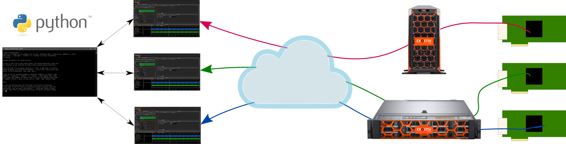
With Exostiv Blade you get massive and actionable visibility into FPGAs to boost your prototyping strategy and deliver IP with confidence.
As always, thank you for reading.
– Frederic
Recommended read: ‘Deep Cycles’, Brian Dickman and Joe Convey.